- 您现在的位置:买卖IC网 > Sheet目录378 > 2V7002WT1G (ON Semiconductor)MOSFET N-CH 60V 310MA SC70-3
�� �
�
�2N7002W,� 2V7002W�
�Small� Signal� MOSFET�
�60� V,� 340� mA,� Single,� N� ?� Channel,� SC� ?� 70�
�Features�
�?� ESD� Protected�
�?� Low� R� DS(on)�
�?� Small� Footprint� Surface� Mount� Package�
�?� These� Devices� are� Pb� ?� Free,� Halogen� Free/BFR� Free� and� are� RoHS�
�Compliant�
�?� 2V� Prefix� for� Automotive� and� Other� Applications� Requiring� Unique�
�Site� and� Control� Change� Requirements;� AEC� ?� Q101� Qualified� and�
�PPAP� Capable�
�V� (BR)DSS�
�60� V�
�http://onsemi.com�
�R� DS(on)� MAX�
�1.6� W� @� 10� V�
�2.5� W� @� 4.5� V�
�I� D� MAX�
�(Note� 1)�
�340� mA�
�Applications�
�?� Low� Side� Load� Switch�
�?� Level� Shift� Circuits�
�?� DC� ?� DC� Converter�
�?� Portable� Applications� i.e.� DSC,� PDA,� Cell� Phone,� etc.�
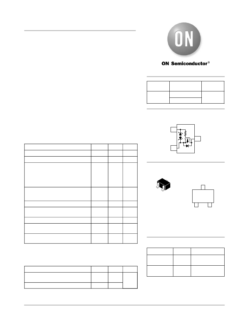
�SIMPLIFIED� SCHEMATIC�
�Gate� 1�
�MAXIMUM� RATINGS� (T� J� =� 25� °� C� unless� otherwise� stated)�
�3�
�Drain�
�Rating�
�Drain� ?� to� ?� Source� Voltage�
�Gate� ?� to� ?� Source� Voltage�
�Symbol�
�V� DSS�
�V� GS�
�Value�
�60�
�±� 20�
�Unit�
�V�
�V�
�Source�
�2�
�(Top� View)�
�Drain� Current� (Note� 1)�
�Steady� State�
�t<5s�
�T� A� =� 25� °� C�
�T� A� =� 85� °� C�
�T� A� =� 25� °� C�
�T� A� =� 85� °� C�
�I� D�
�310�
�220�
�340�
�240�
�mA�
�MARKING� DIAGRAM�
�&� PIN� ASSIGNMENT�
�Drain�
�3�
�Power� Dissipation� (Note� 1)�
�Steady� State�
�t<5s�
�Pulsed� Drain� Current� (t� p� =� 10� m� s)�
�Operating� Junction� and� Storage�
�Temperature� Range�
�P� D�
�I� DM�
�T� J� ,� T� STG�
�280�
�330�
�1.4�
�?� 55� to�
�+150�
�mW�
�A�
�°� C�
�SC� ?� 70/SOT� ?� 323�
�CASE� 419�
�STYLE� 8�
�1�
�Gate�
�71� M� G�
�G�
�2�
�Source�
�Source� Current� (Body� Diode)�
�Lead� Temperature� for� Soldering� Purposes�
�(1/8� ″� from� case� for� 10� s)�
�I� S�
�T� L�
�250�
�260�
�mA�
�°� C�
�71� =� Device� Code�
�M� =� Date� Code�
�G� =� Pb� ?� Free� Package�
�(Note:� Microdot� may� be� in� either� location)�
�Gate� ?� Source� ESD� Rating� ESD� 900� V�
�(HBM,� Method� 3015)�
�Stresses� exceeding� Maximum� Ratings� may� damage� the� device.� Maximum�
�Ratings� are� stress� ratings� only.� Functional� operation� above� the� Recommended�
�Operating� Conditions� is� not� implied.� Extended� exposure� to� stresses� above� the�
�Recommended� Operating� Conditions� may� affect� device� reliability.�
�THERMAL� CHARACTERISTICS�
�Characteristic� Symbol� Max� Unit�
�Junction� ?� to� ?� Ambient� ?� Steady� State� R� q� JA� 450� °� C/W�
�(Note� 1)�
�Junction� ?� to� ?� Ambient� ?� t� ≤� 5� s� (Note� 1)� R� q� JA� 375�
�1.� Surface� ?� mounted� on� FR4� board� using� 1� in� sq� pad� size� (Cu� area� =� 1.127� in�
�sq� [1� oz]� including� traces)�
�ORDERING� INFORMATION�
�Device� Package� Shipping� ?�
�2N7002WT1G� SC� ?� 70� 3000/Tape� &� Reel�
�(Pb� ?� Free)�
�2V7002WT1G� SC� ?� 70� 3000/Tape� &� Reel�
�(Pb� ?� Free)�
�?For� information� on� tape� and� reel� specifications,�
�including� part� orientation� and� tape� sizes,� please�
�refer� to� our� Tape� and� Reel� Packaging� Specifications�
�Brochure,� BRD8011/D.�
�?� Semiconductor� Components� Industries,� LLC,� 2012�
�September,� 2012� ?� Rev.� 5�
�1�
�Publication� Order� Number:�
�2N7002W/D�
�发布紧急采购,3分钟左右您将得到回复。
相关PDF资料
30 PSI-G-4V
SENSOR 30PSIG 4V DUAL
3003308
SHIELDING TAPE COPPER 8MMX33M
3003310
SHIELDING TAPE COPPER 10MMX33M
3003320
SHIELDING TAPE COPPER 20MMX33M
3003325
SHIELDING TAPE COPPER 25MMX33M
3003350
SHIELDING TAPE COPPER 50MMX33M
3013308
SHIELDING TAPE ALUM 8MMX33M
3013310
SHIELDING TAPE ALUM 10MMX33M
相关代理商/技术参数
2V7BC
制造商:SEMTECH_ELEC 制造商全称:SEMTECH ELECTRONICS LTD. 功能描述:Silicon Epitaxial Planar Zener Diodes
2V7BCA
制造商:SEMTECH_ELEC 制造商全称:SEMTECH ELECTRONICS LTD. 功能描述:Silicon Epitaxial Planar Zener Diodes
2V7BCB
制造商:SEMTECH_ELEC 制造商全称:SEMTECH ELECTRONICS LTD. 功能描述:Silicon Epitaxial Planar Zener Diodes
2V7BS
制造商:SEMTECH_ELEC 制造商全称:SEMTECH ELECTRONICS LTD. 功能描述:SILICON PLANAR ZENER DIODES
2V7BSA
制造商:SEMTECH_ELEC 制造商全称:SEMTECH ELECTRONICS LTD. 功能描述:SILICON PLANAR ZENER DIODES
2V7BSB
制造商:SEMTECH_ELEC 制造商全称:SEMTECH ELECTRONICS LTD. 功能描述:SILICON PLANAR ZENER DIODES
2V7HC
制造商:SEMTECH_ELEC 制造商全称:SEMTECH ELECTRONICS LTD. 功能描述:SILICON PLANAR ZENER DIODES
2V7HCA
制造商:SEMTECH_ELEC 制造商全称:SEMTECH ELECTRONICS LTD. 功能描述:SILICON PLANAR ZENER DIODES